|

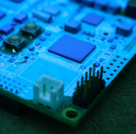
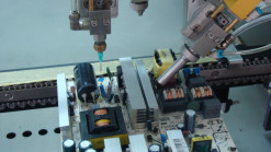
With the use of electronic controls in a wide range of applications, including aerospace, automotive, electrical/white goods, consumer electronics, defense, industrial control, and medical, electronic technology continues to grow in today's products. Due to the fierce competition in the market and strict safety and quality requirements, many application fields are constantly seeking new cost-effective electronic circuit technology to provide better reliability and performance. Printed circuit boards (PCBs) are by far the most common method of assembling modern electronic circuits. Printed circuit boards (PCBs) are the basis for interconnection and packaging for any electronic circuit. The global PCB industry is expected to reach US$93.9 billion in 2017, with an average compound annual growth rate of 8.1%. Demand for smartphones and touch-screen tablets is forecast to grow rapidly. However, due to the product's more compatibility and higher performance requirements, while reducing production costs, the industry is under tremendous pressure. PCB designers and manufacturers face the challenge of more miniaturized and complex board design and manufacturing. The designer's task is to solve complex interconnect-related problems, parasitic components, grounding schemes, and signal decoupling in a limited space on the substrate. Other difficulties associated with designing and fabricating these substrates are the ever-increasing number of chip pins, the development of high-speed serial data streaming techniques, the use of bus interfaces, and the ever-increasing demands of clock rates above 400 MHz. In addition to the above complexities, PCB manufacturers and assemblers are also striving to improve the reliability of printed circuit boards. Improving the surface treatment of bare PCBs, protecting the copper surface from oxidation, and preserving ubiquitous corrosion have been the driving forces behind the industry. To meet these tough challenges, Semblant has developed nano-coated polymers and plasma polymer materials to meet the current and future needs of the industry. Below we will report some of the test properties of our coated films, demonstrating their ability to solve the most difficult problems in a variety of printed circuit board applications. Plasma polymerization is a surface treatment technique that forms a polymer material under the influence of a plasma (partially ionized gas) which is generated by a discharge. In general, the plasma polymer film is no more than a few microns thick and has the following characteristics: • Highly consistent adhesion to a variety of substrates such as glass, metals and conventional polymers. • Highly dense without pinholes. • Polymer films are highly crosslinked. • Multilayer films or films that can easily prepare chemical and physical properties at all levels. • One-step method, contrary to other conventional polymerization techniques. Plasma polymerization is also well suited for functional surface functionalization. For example, by applying a hydrocarbon and a fluorocarbon to a plasma, a crosslinked polymer film having a sufficient functional group can be obtained. The chemical reaction mechanism includes a gas phase process (decomposed by electron collision) and a surface treatment process (association) of film growth. For industrial applications, in addition to the properties of the deposited film, processing speed (ie, deposition rate) and versatility of the processing equipment, as well as scalability to high volume manufacturing are also critical. Therefore, we used production site-proven equipment, 13.56 MHz radio frequency (RF) capacitively coupled discharge, developed and commercialized two types of plasma deposited polymer films for surface finishing and conformal coating in the PCB industry. There is a special report on our process steps and equipment installation/configuration details.
|